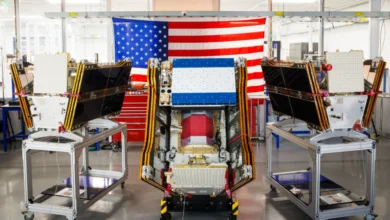
Alphabet Parent Alphabet Developing Custom Frozen v2 AI Server Chips to Enhance Gemini Model Efficiency and Reduce Reliance on Nvidia


The technological landscape of artificial intelligence is currently defined by a frantic race for specialized hardware, and Alphabet, the parent company of Google, has signaled its intent to maintain a leading position through the development of a highly advanced internal server chip. Internally codenamed "Frozen v2," this new silicon architecture is specifically designed to optimize the performance and energy consumption of Google’s proprietary Gemini large language models. According to industry reports, the project represents a significant leap forward in custom hardware engineering, with an anticipated release window set for 2028. This move highlights a broader industry trend where major hyperscalers are increasingly seeking to verticalize their supply chains to mitigate the soaring costs and power demands associated with generative AI.
The Information, citing sources familiar with the project, recently disclosed that Frozen v2 is being engineered to achieve a massive leap in efficiency. Preliminary estimates suggest the chip could be between six and ten times more efficient than Google’s current generation of AI-focused silicon when measured by the number of tokens generated per unit of power. For a company of Alphabet’s scale, where data center operations consume terawatts of electricity, such an improvement in performance-per-watt is not merely a technical milestone but a financial and environmental necessity.
The Strategic Shift Toward Custom Inference Hardware
The development of Frozen v2 comes at a critical juncture for Google. While the company has long been a pioneer in custom silicon—most notably through its Tensor Processing Units (TPUs), which have been in use since 2015—the demands of the "Gemini era" require a more granular approach to hardware-software co-design. Most current AI chips are designed to handle a broad range of tasks, but as models like Gemini 1.5 Pro and Gemini Ultra become more complex, the overhead of general-purpose hardware becomes a bottleneck.
Frozen v2 appears to be targeted specifically at inference—the stage where a trained AI model processes new data to generate responses. As AI moves from the laboratory into widespread consumer and enterprise applications, the volume of inference tasks is expected to dwarf the compute power required for initial model training. By creating a chip optimized for the specific mathematical operations and memory pathways utilized by Gemini, Google aims to provide a faster, more responsive user experience while simultaneously lowering the marginal cost of every query processed by its search engines, Workspace tools, and cloud services.
A Chronology of Google’s Silicon Evolution
To understand the significance of Frozen v2, one must look at Google’s decade-long journey in custom hardware. The company’s foray into silicon began as a clandestine project to solve a specific problem: the realization that if every Android user used voice search for just three minutes a day, Google would need to double its entire data center footprint.
- 2015: The Introduction of TPU v1. Google deployed its first Tensor Processing Units, which were application-specific integrated circuits (ASICs) designed specifically for machine learning inference.
- 2017-2021: Scaling with TPU v2, v3, and v4. These iterations introduced training capabilities and liquid cooling, allowing Google to train increasingly large models like BERT and early versions of PaLM.
- 2023: TPU v5p and the Gemini Launch. Google announced its most powerful TPU to date, the v5p, which was instrumental in training the Gemini family of models. This chip offered significantly better price-performance than its predecessors.
- 2024: Axion and the ARM Expansion. Earlier this year, Google introduced Axion, its first custom ARM-based CPU designed for data centers. Axion was designed to provide high performance for general-purpose workloads, acting as a companion to the specialized AI accelerators.
- 2028 (Projected): Frozen v2. The rumored release of the Frozen v2 chip marks the next phase of this evolution, focusing on extreme efficiency and deep integration with the next generations of Gemini.
Economic Implications and Market Reaction
The financial stakes of this development are enormous. Alphabet has recently communicated to investors that it expects to spend between $180 billion and $190 billion on capital expenditures related to AI infrastructure over the coming years. This "AI bond binge," as some analysts have called it, has created a sense of unease among shareholders who are eager to see a clear path to profitability.
The news of Frozen v2 acted as a catalyst for market optimism. Following the initial reports of the chip’s development, Alphabet’s stock price rose by approximately 3% during Monday morning trading. Investors viewed the development as a sign that Google is proactively addressing the two biggest threats to its AI margins: the high cost of third-party hardware and the rising price of energy.
By developing Frozen v2, Google is essentially building an insurance policy against the market dominance of Nvidia. Currently, Nvidia’s H100 and upcoming Blackwell B200 GPUs are the gold standard for AI compute, but they come with high price tags and long lead times. Furthermore, Nvidia’s hardware is designed to be versatile enough for any company’s model. Google’s thesis is that a chip designed only for Google’s models will always outperform a general-purpose chip on a cost-per-token basis.
Comparative Landscape: The Industry-Wide Move to Custom Silicon
Google is not alone in its quest for hardware independence. The entire "Magnificent Seven" and several prominent AI startups are currently engaged in a silicon arms race.
- OpenAI: In June, it was revealed that OpenAI is developing its first custom chip, an inference processor nicknamed "Jalapeño," in collaboration with Broadcom and Marvell. This move is seen as essential for OpenAI to scale its services without being entirely beholden to Microsoft’s Azure hardware or Nvidia’s supply chain.
- Anthropic: Recent reports suggest that Anthropic, the creator of the Claude models, is in discussions with Samsung to develop custom silicon, emphasizing the need for hardware that can handle their specific "Constitutional AI" training methods.
- Meta: Mark Zuckerberg’s company has already deployed its Meta Training and Inference Accelerator (MTIA), which helps power the recommendation algorithms for Facebook and Instagram.
- Amazon: Through its AWS division, Amazon has been a leader in the cloud-chip space with its Trainium and Inferentia lines, offering customers an alternative to traditional GPU instances.
The "Frozen v2" project places Alphabet in direct competition with these initiatives, but with the added advantage of Google’s deep vertical integration. Google controls the model (Gemini), the framework (TensorFlow/JAX), the cloud platform (Google Cloud), and the hardware (TPU/Frozen).
Official Responses and Rigorous Exploration
When asked for comment regarding the Frozen v2 report, Google provided a statement that emphasized its commitment to innovation without confirming specific product timelines. "Our teams are constantly researching and experimenting with new innovations to deliver maximum performance and efficiency for our users and customers," a Google spokesperson told TechCrunch. "While not every project moves into production, this rigorous exploration is central to our full stack approach. By co-designing our hardware and software from the ground up, we ensure our systems are integrated and highly optimized for real-world workloads."
This response reflects a cautious corporate strategy. In the semiconductor world, a project slated for 2028 is still in its formative stages. Design choices made today must anticipate the state of AI architecture four years from now—a difficult task in a field where model structures change monthly. However, the mention of a "full stack approach" reinforces the company’s belief that the future of AI lies in the tight coupling of silicon and software.
Analysis of Broader Impact: Energy, Sustainability, and Geopolitics
The pursuit of 6x to 10x efficiency gains is not just about the bottom line; it is also about the physical limits of the power grid. Data centers are currently estimated to consume about 1-2% of global electricity, a figure that could rise significantly by the end of the decade. As tech giants face increasing pressure to meet net-zero carbon goals, the ability to generate more AI output with less electricity is the only way to scale sustainably.
Furthermore, the development of Frozen v2 has geopolitical implications. By designing its own chips, Alphabet reduces its vulnerability to international supply chain disruptions. While Google will still rely on foundries like TSMC or Samsung to manufacture the chips, owning the intellectual property (IP) allows the company to pivot more quickly and customize its hardware for specific regional data center requirements.
The 2028 timeline also suggests that Frozen v2 will likely leverage the next generation of lithography. By the time this chip enters mass production, the industry will have moved toward 2-nanometer or even more advanced process nodes. This suggests that Google is planning for a long-term architectural shift rather than a minor iterative update.
Conclusion: The Road to 2028
The development of the Frozen v2 chip is a clear indication that Alphabet views AI not as a temporary trend, but as the foundational pillar of its future business. By investing in custom silicon that promises an order-of-magnitude increase in efficiency, Google is positioning itself to win the "war of attrition" in the AI sector—where the winner is not just the one with the best model, but the one who can run that model at the lowest cost and highest scale.
While 2028 remains a distant horizon in the fast-moving world of technology, the roadmap for Frozen v2 provides a glimpse into a future where AI is ubiquitous, energy-efficient, and powered by highly specialized "bespoke" silicon. For investors, the project offers a measure of reassurance that Google’s massive capital expenditures are being directed toward a sustainable, high-margin future. For the broader industry, it serves as a reminder that the battle for AI supremacy will be fought as much in the silicon foundries as in the coding of neural networks.
Related posts: