Microsoft Accelerates Silicon Innovation with the Deployment of Azure Cobalt 200 for EDA Workloads


The rapid evolution of semiconductor design, fueled by the insatiable demand for AI-capable hardware and high-performance computing, has necessitated a fundamental shift in how silicon is engineered. Microsoft has announced a significant milestone in this domain, revealing that its next-generation Azure Cobalt 200 infrastructure—built on the Arm Neoverse CSS V3 architecture—is now delivering substantial performance gains for electronic design automation (EDA) workloads. By transitioning from traditional, fixed-capacity on-premise x86 servers to cloud-native environments, Microsoft’s silicon design teams have unlocked new efficiencies, enabling them to validate, simulate, and finalize complex chips with unprecedented speed.
The move to Cobalt 200 represents more than a simple hardware refresh; it is a strategic architectural evolution. EDA jobs—which range from multi-day simulation sweeps to massive verification regressions spanning thousands of cores—are notoriously resource-intensive. Historically, these workloads were constrained by the physical limits of on-premise data centers, which often required massive capital expenditure to accommodate peak demand, only to sit underutilized during off-peak cycles. The cloud-based approach allows for elastic scaling, where compute power is provisioned on demand, ensuring that engineering teams are never throttled by infrastructure limitations.

A Chronology of Cloud-Driven Silicon Design
The journey toward this performance breakthrough began years ago as Microsoft transitioned its internal silicon development workflows from legacy hardware to the Azure cloud. This shift was not merely about migration but about re-engineering the development pipeline to be "cloud-first."
In the early stages of this transition, Microsoft utilized initial iterations of cloud infrastructure to handle basic RTL (Register Transfer Level) simulations. As the complexity of Microsoft’s custom silicon—such as the Azure Cobalt line—grew, the need for a more specialized compute environment became apparent. The introduction of Cobalt 100 served as the first major step in creating a bespoke silicon environment optimized for the specific, highly parallelized needs of EDA tools.
Following the success of Cobalt 100, the engineering teams began evaluating the Arm Neoverse CSS V3 platform. Throughout 2024 and early 2025, internal tests were conducted to measure how the Cobalt 200 architecture handled the unique memory and compute demands of EDA software. The results, finalized in late 2025 and released in current reports, confirm a significant leap in generational performance. This timeline reflects a deliberate strategy: using custom-built cloud silicon to design the next generation of cloud-ready silicon, creating a self-sustaining cycle of innovation.
Performance Benchmarks and Technical Architecture
The performance gains observed in Cobalt 200 are rooted in its fundamental architecture. Unlike systems that rely on hyperthreading—which can introduce latency and resource contention in heavily loaded environments—Cobalt 200 utilizes dedicated physical cores. Each core is paired with a generous 3MB L2 cache and high-provisioned memory bandwidth, providing the predictable throughput required by computer-aided design (CAD) managers who must plan complex overnight regressions.
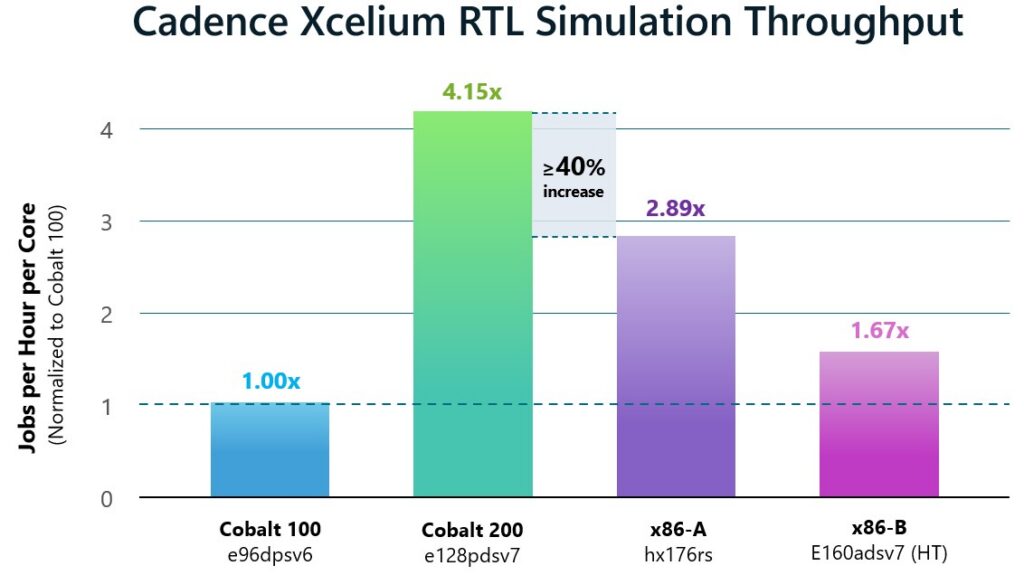
In rigorous comparative testing, the Cobalt 200 system demonstrated performance improvements ranging from 1.30x to 4.15x over the Cobalt 100 platform across a spectrum of industry-standard EDA tools, including Cadence Xcelium, Cadence Spectre, Synopsys PrimeTime, Synopsys VCS, and Siemens Calibre.
For digital simulation, which is the cornerstone of functional verification, the Cobalt 200 proved superior. In testing using Cadence Xcelium and Synopsys VCS, the new infrastructure delivered more than 40% higher throughput per logical core compared to any other system in the test suite, including high-performance x86 alternatives. This is critical for teams running large-scale regression suites where every percentage point of efficiency translates into hours of time saved per design cycle.
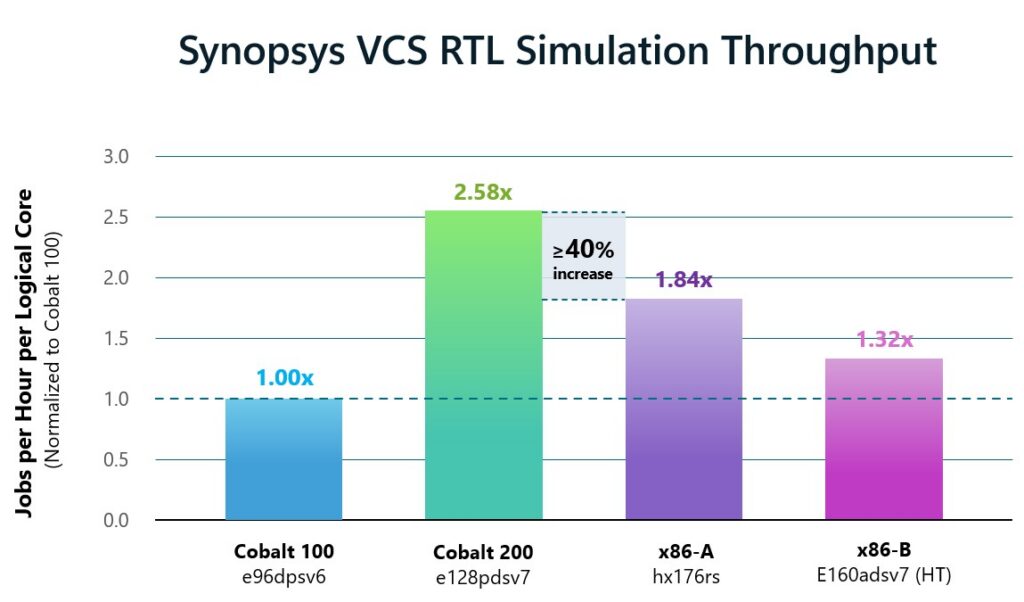
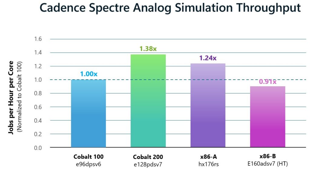
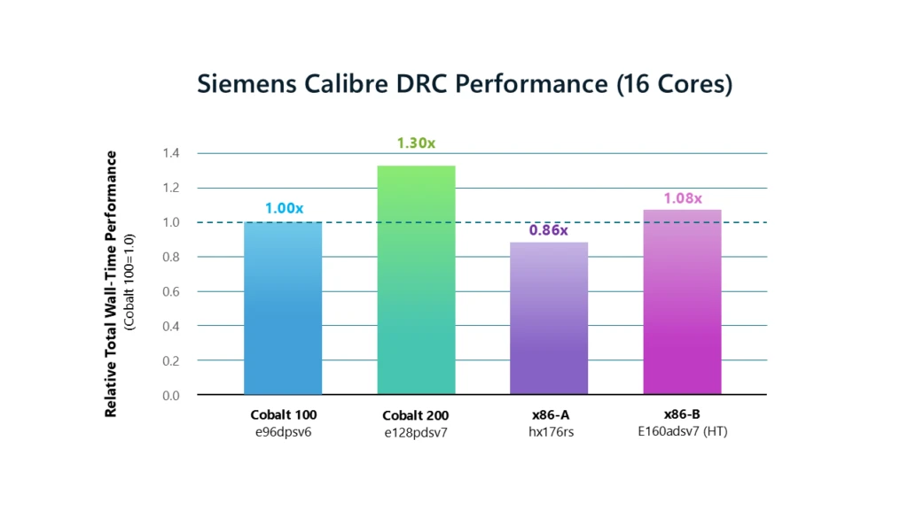
Analog and mixed-signal simulations, which are notoriously difficult to parallelize, also saw significant gains. Cadence Spectre, when running on Cobalt 200, achieved 38% higher throughput compared to the previous generation, outperforming competitive x86 Azure VMs. In the realm of physical verification—specifically Siemens Calibre DRC (Design Rule Checking) tasks—the system achieved a 23% reduction in wall time, allowing for faster iterations of physical layouts. Finally, static timing analysis using Synopsys PrimeTime saw a 2x increase in peak throughput per logical core, confirming the platform’s ability to handle the most demanding verification stages of the tapeout process.
Industry Collaboration and Ecosystem Impact
The validation of the Cobalt 200 platform was not conducted in isolation. Microsoft engaged deeply with key EDA partners to ensure that software tools functioned seamlessly on the new architecture. Because the tools enabled on Cobalt 100 were compatible with the newer generation, Microsoft was able to focus entirely on performance optimization rather than basic functionality, a testament to the stability of the Arm-based software ecosystem in the cloud.
Industry leaders have been vocal about the implications of this partnership. Paul Cunningham, Senior Vice President and General Manager of the System Verification Group at Cadence, noted that the collaboration allows semiconductor teams to exercise greater flexibility in how they access and scale compute. Similarly, Craig Johnson, VP of Cloud Solutions at Siemens EDA, highlighted that matching the right workloads to the right compute architecture is the defining challenge for modern silicon innovation.
Sanjay Bali, Senior Vice President of EDA Product Management and Strategy at Synopsys, emphasized the generational progress, citing the 40% faster runtimes with Synopsys VCS as a pivotal achievement. These statements underscore a broader industry consensus: the future of semiconductor design is inextricably linked to the availability of specialized, high-performance cloud infrastructure.
Broader Implications for the Semiconductor Industry
The success of the Azure Cobalt 200 platform carries significant implications for the broader semiconductor industry. First, it proves that Arm-based server infrastructure is not only viable but superior for high-concurrency, memory-intensive EDA tasks that were once considered the exclusive domain of traditional x86 server farms. This shift may trigger a wider migration of EDA workflows to cloud environments, as firms look to replicate Microsoft’s efficiency gains.
Second, the "virtuous cycle" of using custom cloud silicon to design future generations of that same silicon suggests a tightening of the development lifecycle. Companies that can leverage cloud-based EDA effectively will likely see faster time-to-market for their products, creating a competitive divide in the industry. As chips grow in complexity—incorporating more transistors, specialized AI accelerators, and heterogeneous compute blocks—the infrastructure used to design them becomes a primary bottleneck. By removing this bottleneck, Microsoft is effectively lowering the barrier to entry for complex, high-performance silicon design.
Finally, the focus on platform-level advantages—such as storage, data movement, and high-bandwidth interconnects—highlights that raw compute power is only one part of the equation. Microsoft’s ability to pair the Cobalt 200 compute with robust, scalable storage solutions demonstrates an understanding of the end-to-end silicon lifecycle.
Future Outlook and Next Steps
As Cobalt 200 moves toward general availability, Microsoft has signaled that it intends to broaden the scope of its testing and continue collaborating with EDA partners to further tune the software stack. The goal is to ensure that as the platform scales, the performance gains remain consistent across even larger, more complex design projects.
For semiconductor engineering teams, the data presented provides a clear roadmap for the future of cloud-based design. The transition from legacy, static hardware to the flexible, high-performance environment of Azure Cobalt 200 is not just an incremental update; it is a fundamental reconfiguration of the silicon development paradigm. As the industry continues to push the boundaries of what is possible in chip design, the underlying infrastructure will play an increasingly vital role in turning theoretical designs into physical, high-performance reality. Microsoft’s early results with Cobalt 200 offer a compelling preview of this transition, setting a new benchmark for speed, efficiency, and scalability in the semiconductor sector.
Related posts: