Azure Cobalt 200 Delivers Significant Performance Gains for Electronic Design Automation Workloads


The semiconductor industry is currently undergoing a structural shift, moving away from traditional, on-premise, fixed-capacity server farms toward the elastic, high-performance environment of the cloud. Central to this transformation is the evolution of electronic design automation (EDA)—the software suite of choice for designing, testing, and validating complex silicon chips. Microsoft has recently unveiled early performance data for its Azure Cobalt 200 virtual machines (VMs), which are built on the Arm Neoverse CSS V3 architecture. These results suggest that the next generation of cloud infrastructure is uniquely positioned to handle the massive compute demands of modern chip design, offering performance improvements ranging from 30% to over 400% compared to previous generations and established x86 alternatives.
Every custom chip Microsoft has developed—including its own Cobalt and Maia series—relies on EDA workflows. These processes involve simulation sweeps that can last for days, verification regressions that necessitate thousands of concurrent compute cores overnight, and physical signoff runs that demand hundreds of gigabytes of memory for a single block. Given that Microsoft’s internal silicon engineering teams process hundreds of millions of compute jobs annually, even incremental improvements in performance translate into massive gains in development velocity and cost efficiency.
A Chronological Shift in Silicon Design Infrastructure
Historically, semiconductor companies were tethered to physical, on-premise data centers. These facilities were typically sized to accommodate "peak demand"—the maximum capacity required during the final, most intensive stages of a chip’s development, such as tapeout. This model inevitably led to long periods of underutilization, where expensive hardware sat idle during the quieter phases of the design cycle.

The shift to Microsoft Azure began as a strategic move to optimize this cycle. By adopting cloud-based EDA, teams gained the ability to scale compute resources instantly to meet project milestones and release those resources the moment a job was completed. The introduction of the original Azure Cobalt 100 was the first step in this journey, establishing that Arm-based server infrastructure could handle the complex, multi-threaded nature of EDA tools without requiring modifications to existing codebases.
The transition from Cobalt 100 to Cobalt 200 represents the second, more aggressive phase of this evolution. By optimizing for specific EDA characteristics—such as the requirement for large L2 caches and high memory bandwidth—Microsoft has tailored the Cobalt 200 platform to meet the specific "throughput-per-core" needs that dictate how quickly a CAD manager can finalize a design.
Performance Benchmarks and Data Analysis
The evaluation of Cobalt 200 focused on the most critical components of the EDA flow: RTL simulation, gate-level simulation, static timing analysis (STA), and physical verification. To ensure a fair comparison, Microsoft normalized throughput on a per-logical-core basis, comparing the Cobalt 200 against its predecessor, the Cobalt 100, and standard high-performance x86-based Azure VMs.
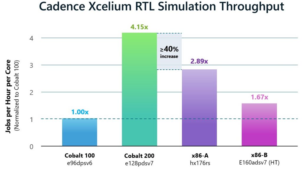
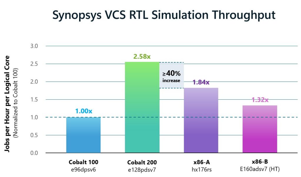
In the realm of digital simulation, which utilizes industry-standard tools like Cadence Xcelium and Synopsys VCS, the results were particularly stark. Cobalt 200 demonstrated a 40% improvement in peak throughput per logical core over any other tested system. This is a critical metric for engineering teams, as functional verification is often the most time-consuming stage of the development cycle. By accelerating these simulations, companies can run more regression tests in a shorter window, significantly reducing the "time-to-market" for new silicon.
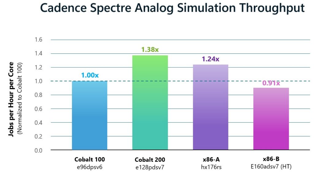
Analog and mixed-signal simulations, tested using Cadence Spectre, also showed marked improvements. Unlike digital simulation, which is highly parallelizable, analog simulation is often limited by multithreaded performance. Cobalt 200 delivered 38% higher throughput generation-over-generation, outperforming comparable x86 configurations by 11% to 52%.
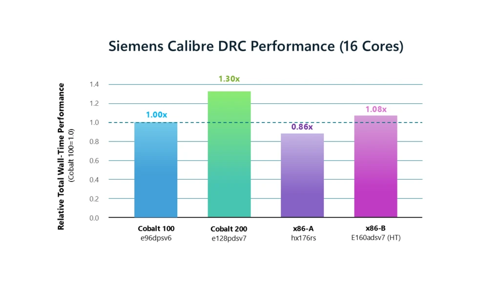
Static timing analysis, performed via Synopsys PrimeTime, showed a twofold (2x) improvement in peak throughput compared to Cobalt 100. This analysis is vital for ensuring that a chip meets its frequency requirements. Finally, for physical verification—the final check before a design is sent for manufacturing—the Siemens Calibre toolset running on Cobalt 200 achieved a 23% reduction in wall-clock time compared to the previous generation, proving that the architecture is not just faster at computation, but also more efficient at managing large-scale data handling.
Technical Drivers of Success
The performance gains in Cobalt 200 are not incidental; they are the result of specific hardware architectural choices. EDA workloads are notoriously memory-intensive and sensitive to cache latency. When hundreds of jobs run concurrently, the system’s ability to move data between the CPU and memory without bottlenecking is paramount.
Cobalt 200 features a dedicated 3MB L2 cache per core and utilizes an architecture that removes the overhead associated with hyperthreading. In many standard cloud workloads, hyperthreading allows for better utilization of hardware, but in the highly sensitive and deterministic world of EDA, it can lead to "noisy neighbor" effects and unpredictable performance. By focusing on physical cores and providing a generous cache hierarchy, Microsoft has ensured that EDA jobs run with high predictability, which is a requirement for CAD managers planning massive overnight regressions.
Industry Perspectives and Partnerships
The success of the Cobalt 200 platform relies heavily on the ecosystem of EDA providers. Because the Cobalt 200 environment supports tools like Cadence, Synopsys, and Siemens without requiring modifications, the migration path for semiconductor companies is essentially seamless.
Industry leaders have expressed optimism regarding this development. Paul Cunningham, Senior Vice President and General Manager of the System Verification Group at Cadence, noted that the collaboration between Cadence and Microsoft on Cobalt spans multiple generations of silicon. He highlighted that the qualification of Cadence workflows on Cobalt 200 provides semiconductor teams with the necessary flexibility to scale their compute resources precisely when needed.
Craig Johnson, Vice President of Cloud Solutions at Siemens EDA, echoed these sentiments, emphasizing that as semiconductor designs grow increasingly complex—driven by the demands of AI and advanced computing—the ability to match specific workloads to optimized compute architectures is becoming a competitive necessity.
Sanjay Bali, Senior Vice President of EDA Product Management and Strategy at Synopsys, provided a quantitative validation of these partnerships. He highlighted the "meaningful performance gains," specifically pointing to the 40% faster runtimes with Synopsys VCS and the 2x per-core throughput with Synopsys PrimeTime. These improvements are critical for the next generation of AI silicon, which requires more iterations and more rigorous verification than traditional chip architectures.
Broader Implications for the Semiconductor Sector
The successful deployment of Cobalt 200 signals a broader trend in the cloud-computing industry: the rise of specialized, workload-optimized silicon. For years, the cloud was a "one-size-fits-all" environment dominated by general-purpose x86 processors. As the demand for custom silicon grows—fueled by the AI boom—the cloud providers themselves are becoming the largest users of EDA tools, effectively creating a "virtuous cycle."
By using EDA tools to design Cobalt 200, and then using Cobalt 200 to design the next generation of Azure chips, Microsoft is tightening the feedback loop of hardware development. This approach allows the company to observe real-world performance bottlenecks in the EDA flow and feed that data directly into the design of future compute infrastructure.
For the wider industry, this means that the cloud is no longer just a place to host applications; it is the laboratory where the next generation of processors is being conceived. Companies that are not currently utilizing cloud-based EDA are likely to face significant hurdles as the complexity of chips increases and the need for agile, scalable compute resources becomes even more acute.
Conclusion and Future Outlook
As Cobalt 200 moves toward general availability, the next phase of the project will involve broadening the scope of validated workloads and increasing the scale of deployment. While the initial tests have been overwhelmingly positive, the long-term impact will be measured by how well this platform handles the diverse, unpredictable demands of global semiconductor firms.
Microsoft has positioned the Cobalt 200 not just as an incremental upgrade, but as a fundamental shift in how the most compute-intensive processes in the world are handled. By removing the constraints of physical, fixed-capacity infrastructure and replacing them with high-performance, Arm-based cloud resources, Microsoft is lowering the barrier to entry for advanced chip design. For the engineering teams responsible for the next wave of silicon innovation, the promise of higher throughput and more predictable performance is likely to be a deciding factor in their transition to the cloud.